

半导体设计培训中心(IDEC)成立于1995年,由工业和资源部支持成立。通过支持和培训全国大学参与性教授,培养优秀的设计人才,研究中心正在推动一项旨在提高工业基础薄弱的非记忆领域国家竞争力的项目。
研究中心提供制造芯片的环境和实践机会,通过最新的 EDA工具支持构建大学的系统半导体设计环境。随着时代的变化,主动运行教育系统,建立系统化、多方向的信息网络,快速获取信息并鼓励专利和知识产权开发,为高价值创造机会。
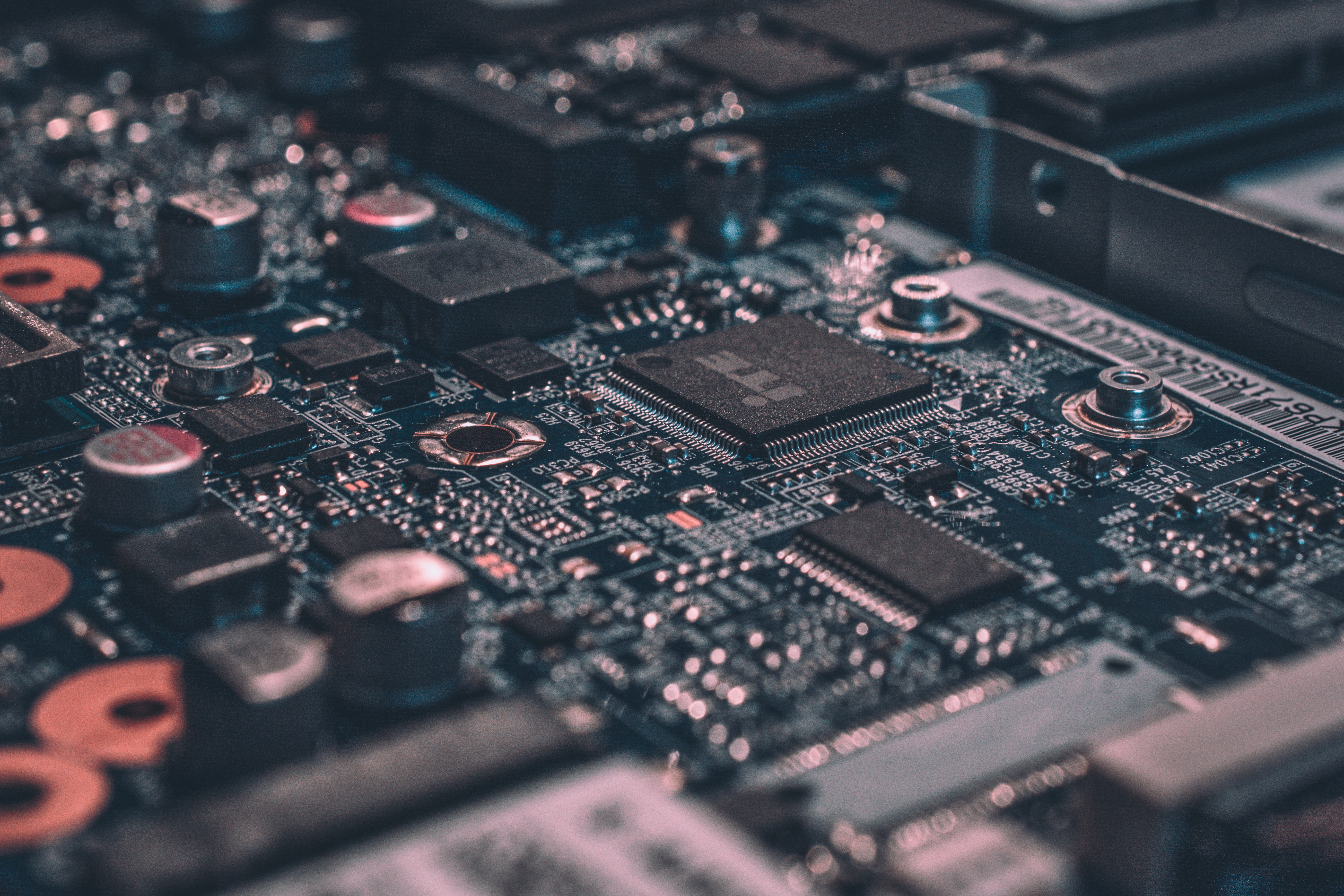
系统半导体是指将存储器、处理器、软件等个别半导体合二为一,控制、运营电子设备系统的半导体。系统半导体是一个集各种电子控制技术于一体的系统,其优点是难以被别人开发,并且能够根据企业的需求或情况配置功能或控制方法。在半导体领域,它与存储和读取信息的存储器半导体不同,因此也被称为非存储器半导体。系统半导体负责计算和多媒体功能等核心功能,不仅包括电子产品,还进入汽车、重工业等电子控制功能,年均增长6%~15%。
IDEC设有ASIC设计室,通过ASIC设计室提供 EDA工具,为未拥有设计环境的大学提供了更多使用EDA工具的机会。Chip设计器为参与MPW提供了大量帮助,因为它减轻了安装EDA工具和设计工具的负担,使他们能够在短时间内专注于设计。
The Semiconductor Design Training Center (IDEC) was established in 1995 with the support of the Ministry of Industry and Resources. By supporting and training participatory professors at universities across the country and nurturing outstanding design talent, the Research Center is promoting a project aimed at improving national competitiveness in non-memory areas with a weak industrial base.
The research center provides an environment and hands-on opportunities for manufacturing chips, supporting the construction of the university's system semiconductor design environment through the latest EDA tools. As the times change, actively operate the education system, establish a systematic and multi-directional information network, quickly access information and encourage patent and intellectual property development, and create opportunities for high value.
System semiconductors are semiconductors that combine individual semiconductors such as memory, processor, and software into one to control and operate electronic equipment systems. System semiconductor is a system that integrates various electronic control technologies, and its advantage is that it is difficult to be developed by others, and it can configure functions or control methods according to the needs or situations of the enterprise. In the field of semiconductors, it is different from memory semiconductors that store and read information, so it is also called non-memory semiconductors. System semiconductors are responsible for core functions such as computing and multimedia functions, including not only electronic products, but also electronic control functions such as automobiles and heavy industry, with an average annual growth of 6%~15%.
IDEC has an ASIC design room, through which EDA tools are available, providing more opportunities for universities that do not have a design environment to use EDA tools. Chip Designer provides a lot of help in participating in MPWs as it eases the burden of installing EDA tools and design tools, allowing them to focus on design in a short period of time.