创新背景
在斯坦福大学上方的山坡上,SLAC国家加速器实验室运行着一个近2英里长的科学仪器。在这个巨大的加速器中,随着微波辐射的爆发,电子流通过真空管,推动粒子以越来越快的速度向前移动,直到它们的速度接近光速,形成强大的光束,来自世界各地的科学家用来探测无机和生物材料的原子和分子结构。
正如工程师们曾经将房间大小的大型机的部分功能压缩到台式电脑上一样,斯坦福大学的研究人员也尝试将巨大粒子加速器的部分功能压缩到一个微型硅芯片上。
创新过程
斯坦福大学和SLAC的科学家们发明了一种硅芯片,它可以加速电子,尽管速度远比不上庞大的仪器——使用红外激光在不到一根头发宽度的范围内,提供微波需要许多英尺的能量提升。
研究人员计划从硅中雕刻出一个纳米级的通道,将它密封在真空中,并将电子通过这个空腔,同时红外光脉冲通过通道壁传输,以加快电子的速度。硅对红外光的透明度就像玻璃对可见光的透明度一样。
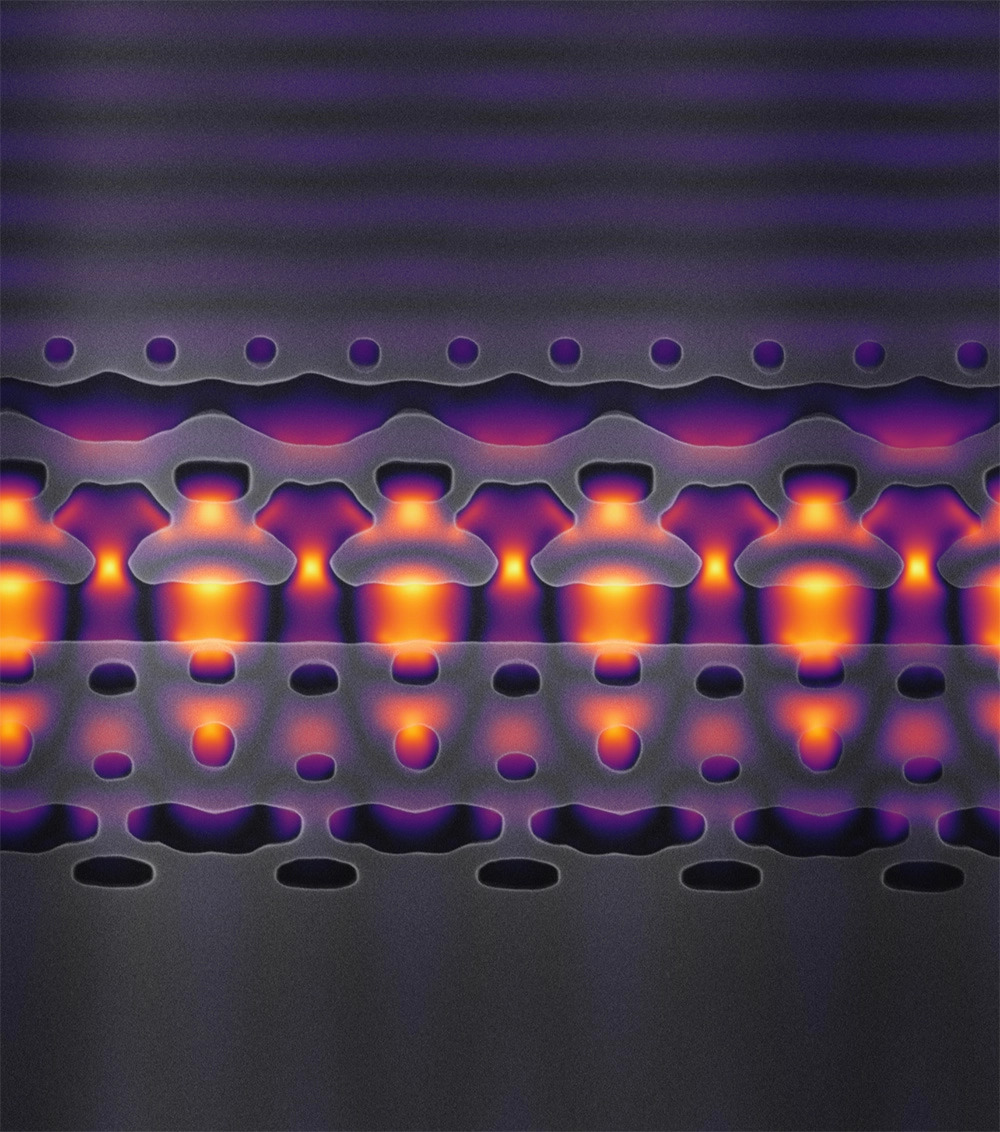
这幅放大了25,000倍的图像显示了芯片加速器的一部分。灰色结构将红外激光(以黄色和紫色显示)聚焦在流经中心通道的电子上。通过将1000个通道封装到一英寸大小的芯片上,有希望将电子加速到光速的94%。
为了实现这一目标,他们将设计过程颠倒过来。在传统的加速器中,工程师们通常会先草拟一个基本设计,然后运行模拟,在物理上安排微波爆发,以提供可能的最大加速度。但是微波从峰值到波谷的长度是4英寸,而红外光的波长只有人类头发宽度的十分之一。这种差异解释了为什么与微波相比,红外光可以在如此短的距离内加速电子。但这也意味着该芯片的物理特性必须比传统加速器中的铜结构小10万倍。这就需要一种基于硅集成光子学和光刻技术的新工程方法。
研究团队使用逆向设计算法解决了这个问题。这些算法允许研究人员反向工作,通过指定他们希望芯片传递多少光能,并给软件分配任务,建议如何构建合适的纳米级结构,以使光子与电子流进行适当的接触。
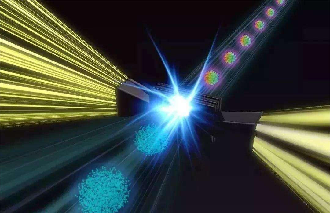
设计算法提出了一个芯片布局:纳米级别的台面,被硅蚀刻的通道隔开。通过通道的电子穿过硅线,在峡谷壁的重要位置戳出。每一次激光脉冲(每秒10万次)都会有一束光子撞击一堆电子,加速它们向前移动。所有这一切都发生在斯坦福大学团队成员制作的真空密封硅芯片的表面上,其宽度小于头发的宽度。
研究人员希望将电子加速到光速的94%,或100万电子伏(1MeV),以创造出足以用于研究或医疗目的的粒子流。这个原型芯片只提供一个阶段的加速,电子流必须通过大约1000个阶段才能达到1MeV。这个芯片上的加速器原型是一个完全集成的电路。这意味着制造加速所需的所有关键功能都内置在芯片中,增加其功能应该是相当简单的。
创新关键点
研究人员计划从硅中雕刻出一个纳米级的通道,将它密封在真空中,并将电子通过这个空腔,同时红外光脉冲通过通道壁传输,以加快电子的速度。
创新价值
除了研究应用之外,还可以从加速器技术的小型化中获得医疗效益。
例如,医用x光机占据了整个房间,发出的射线很难聚焦在肿瘤上,这就要求患者戴上铅护罩,以减少附带伤害。但新技术可能将电子束辐射直接传递到肿瘤上,而不影响健康组织。
Innovative development of "micro silicon chips" that use infrared lasers to speed up electron movement
Scientists at Stanford University and SLAC have created a silicon chip that speeds up electrons, though not nearly as fast as bulky instruments - using infrared lasers to provide microwaves within less than the width of a human hair requires an energy boost of many feet.
The researchers plan to carve a nanoscale channel out of silicon, seal it in a vacuum and pass electrons through the cavity while pulses of infrared light travel through the channel walls to speed up the electrons. Silicon is as transparent to infrared light as glass is to visible light.
To achieve this, they turned the design process upside down. In traditional accelerators, engineers typically draw up a basic design and then run simulations that physically arrange microwave bursts to provide the maximum possible acceleration. But microwaves span four inches from peak to trough, and infrared light has a wavelength only one-tenth the width of a human hair. This difference explains why infrared light can accelerate electrons over such short distances compared to microwaves. But this also means that the physical properties of the chip must be 100,000 times smaller than the copper structure in a conventional accelerator. This calls for a new engineering approach based on silicon integrated photonics and lithography.
The research team solved the problem using a reverse design algorithm. These algorithms allow researchers to work in reverse, by specifying how much light energy they want the chip to deliver and assigning the software the task of suggesting how to build the right nanoscale structures to make proper contact between photons and the electron flow.
The design algorithm came up with a chip layout: nanoscale mesa, separated by channels etched in silicon. Electrons passing through the channel pass through the silicon wire and poke out at important points in the canyon wall. With each laser pulse (100,000 pulses per second), a beam of photons hits a bunch of electrons, speeding them forward. All this happened on the surface of a vacuum-sealed silicon chip made by members of the Stanford team that is less than the width of a human hair.
Researchers hope to accelerate electrons to 94 percent of the speed of light, or 1 million electron volts (1MeV), to create a stream of particles large enough to be used for research or medical purposes. This prototype chip provides only one stage of acceleration, and the electron flow must pass through about 1,000 stages to reach 1MeV. This prototype accelerator on a chip is a fully integrated circuit. This means that all the key features needed to make the speedup are built into the chip, and adding its capabilities should be fairly straightforward.
智能推荐
化学创新思维 | 微藻分泌物保存核废料的可能
2022-06-29研究微藻分泌物以及其他自然形成物质,挖掘其对核废料封存处理的可能性影响。
涉及学科涉及领域研究方向光纤通信创新思维 | 以高速率进行传输的新型55模光纤
2022-11-22研究人员展示了世界上第一个在任何标准包层直径光纤中以每秒1.53petbtes的创纪录数据速率进行55模式传输。新型55模光纤仅使用最常见的光通信(C-)频段即可实现超高频谱效率和高数据速率。
涉及学科涉及领域研究方向